
XIAMEN NINESUN IMP. & EXP. CO., LTD
China

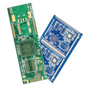
Processing Technology: Electrolytic Foil Base Material: Copper Insulation Materials: Epoxy Resin Certification: UL, RoHS, ISO9001, Ts16949 Transport Package: by Vacuum Packing in Cartons Specification: UL, ROHS, SGS Origin:China HS Code: 85340090 Min. Order: 100 Pieces Port: China Production Capacity:100000 Square Meters Per Month Payment Terms: L/C, T/T, D/P Type: Rigid Circuit Board Dielectric:FR-4 Material: Fiberglass Epoxy Application: Consumer Electronics Flame Retardant Properties: V0 Mechanical Rigid: Rigid
DAMEKS
Poland
PCB depanelization is a process step in the production of large-scale assembly of electronics. To increase the throughput of printed circuit board (PCB) and surface mount (SMT) production lines, printed circuit boards are often designed to consist of many smaller individual printed circuit boards that will be used in the final product. This PCB cluster is called a panel or multi-block. The large panel is broken or "depanellated" as a process step - depending on the product, this can be right after the SMT process, after the in-circuit test (ICT), after soldering through-hole components, and even just before the final assembly of the PCBA in the enclosure.

BLUE CHIP TECHNOLOGY LTD
United Kingdom
Blue Chip Technology have an in-house team of dedicated engineers with a wealth of expertise and experience in designing boards for a variety of applications and industries. We excel in compact PCB designs that allow you to incorporate the necessary features into your product.

DK CERAMIC CIRCUITS
Belgium
LTCC (Low Temperature Co-fired Ceramic) is a multilayer capable substrate technology offering excellent RF and microwave performance characteristics. Thanks to its low sintering temperature (around 900°C) allows it to co-fire with highly conductive metals such as silver and gold. It is sometimes referred to as “glass ceramics” because glass is mixed in its main raw material, alumina. Elite Advanced Technologies is one of the few LTCC specialists globally that is producing its own green tape (base material low temperature co-fired ceramics). LTCC is best suited for applications that can take advantage of one or more of the following: Good electrical performance Dimensional and electrical stability under temperature, moisture and mechanical stress 3D capability curved, cavities, channels Effective thermal management with metal loaded vias (>100 W/MK) Hermeticity Matched TCE with semiconductors (Thermal Coefficient of Expansion) Multiple assembly and packaging solutions
DK CERAMIC CIRCUITS
Belgium
When you are looking for substrates for electronic circuits with a high thermal conductivity and a low expansion coefficient (CTE), ceramic pcb will be your preferred choice of material. Today ceramics are already widely used as substrates in many microelectronic components and power LED packages and more and more they are replacing entire printed circuit boards reducing complexity in design and manufacturing while increasing performance. Examples are Chip-on-board (COB) modules, High power circuits, proximity sensors, battery drivers for EVs, … .

DK CERAMIC CIRCUITS
Belgium
Ceramic prined circuit board feature many advantages over metal core and FR4 circuit boards as they combine excellent thermal characteristics with low a expansion. They are also suitable for multilayer applications, show lower deformation, warpage and operate under higher temperatures. Elite advanced technologies is your partner for ceramic substrates and circuit boards. Thanks to our large laser facilities and patented printing technology we are able to accomodate both very tight tolerances as well as high volume production at a high quality.

GSPK CIRCUITS LTD
United Kingdom
We can make, test and despatch conventional and double-sided plated through hole (PTH) printed circuit boards within 48 hours of receipt of manufacturing data. Provided we receive the data early enough on day one.
INTEGRAL COMPLEX SYSTEMS
Ukraine
We carry out a full cycle of development of electronic devices: supply of electronic components, stencils and printed circuit boards, design of electronics, redesign of finished devices. Applying the principles of lean production, we achieve a price reduction while maintaining a high quality of services. Due to quality control at all stages of production, we have the reject rate less than 0.5% (at observance of all requirements to the order). Operative daily planning allows us to achieve maximum efficiency in the use of working time. Thanks to that, in the presence of all the equipment in the warehouse, we can take the order to work during the day from the moment of order. We have our own high-tech equipment, and offering good quality with competitive assembly cost.

GEPATEK ELEKTRONIK VE SAVUNMA SANAYI AS
Turkey
SMT and THT assembly with automatic lines. IPC Class 1-2-3 products.

XIAMEN NINESUN IMP. & EXP. CO., LTD
China
Origin: China Model Number: JXFPC Min. Hole Size: 0.20mm Materials: PI/PET Type: FPC Layers: 1-6 Finished surface: OSP/ENIG Board thickness: 0.2mm Solder mask color: orange Certificate: ISO9001 Copper weight: 1 OZ Base Material: PI/PET Copper Thickness: 1/2OZ 1OZ 2OZ 3OZ Board Thickness: 0.20mm Min. Line Width: 0.1mm/4mil Min. Line Spacing: 0.1mm/4mil Surface Finishing: OSP/ENIG Supply Ability: 3000 Square Meter/Square Meters per Month Packaging Details: packing with anti-static red/white bubble Port: Xiamen
SHENZHEN PROMOSTAR HARDWARE CO.,LTD
Germany
Electroplating, also known as electrochemical deposition or electrodeposition, is a process that involves coating a solid substrate with a thin layer of metal through the reduction of metal cations using direct electric current.Electroplating is widely used in industry and decorative arts to enhance surface qualities such as abrasion resistance, corrosion resistance, reflectivity, and appearance. It's used to build up thickness on undersized or worn-out parts (electroforming) In electronics, it deposits copper for printed circuit boards and interconnects in integrated circuits. Electroplating can also purify metals like copper.
XIAMEN NINESUN IMP. & EXP. CO., LTD
China
Place of Origin: China Base Material: FR-4 Copper Thickness: 1/2OZ 1OZ 2OZ 3OZ Board Thickness: 0.8mm Min. Hole Size: 0.1mm Min. Line Width: 0.065mm Min. Line Spacing: 0.065mm Surface Finishing: HASL Application: Electronics Device Type: Customizable Solder mask: Black Material: FR4 CEM1 CEM3 height TG Color: Red Blue Green Black Testing Service: 100% Supply Ability: 25000 Square Meter/Square Meters per Month

THERMA THERMOFÜHLER GMBH
Germany
Use: Miniature Jack/Socket for thermocouple and RTD circuits. Designed for direct soldering onto printed circuit boards. This version is suitable for flat mounting other versions available, please see separate specification sheet. Mechanical design: • Housing of fibreglass-filled plastic. • Contacts of original thermocouple materials and • spring-loaded sockets for reliable contact. • Moulded barriers prevent short-circuits. • Reverse polarity protection by different contact pin widths. • One-piece housing withstands great stresses.

THERMA THERMOFÜHLER GMBH
Germany
Use: Miniature Jack/Socket for thermocouple and RTD circuits. Designed for direct soldering onto printed circuit boards. This version is suitable for flat mounting other versions available, please see separate specification sheet. Mechanical design: • Housing of fibreglass-filled plastic. • Contacts of original thermocouple material and spring-loaded sockets for reliable contact. • Moulded barriers prevent short-circuits. • Reverse polarity protection by different contact pin widths. • One-piece housing withstands great stresses.

THERMA THERMOFÜHLER GMBH
Germany
Use: Miniature Jack/Socket for thermocouple and RTD circuits. Designed for direct soldering onto printed circuit boards. This version is suitable for flat mounting other versions available, please see separate specification sheet. Mechanical design: • Housing of fibreglass-filled plastic. • Contacts of original thermocouple materials and spring-loaded sockets for reliable contact. • Reverse polarity protection by different contact pin widths. • One-piece housing withstands great stresses.
DYMAX EUROPE GMBH
Germany
Dymax Dual-Cure 9014 encapsulant is formulated to cure primarily with UV light and includes a secondary moisture curing function for applications where shadow areas exist on printed circuit boards. Features: - Cures with UV/Visible light - Dual Cure secondary moisture cure capability - Fluoresces blue under black lights - Flexible

Do you sell or make similar products?
Sign up to europages and have your products listed

ISOVOLTA AG
Austria
CONTAVAL® 2017 is a laminate consisting of E-glass fabric, graphite and epoxy-resin and is used e. g. as a conductive slot filler in machines and also as soldering bath carriers for printed circuits. CONTAVAL® 2017 has excellent mechanical properties and shows conductivity parallel and perpendicular to the layers as well as high chemical and temperature resistance.
MODUS HIGH-TECH ELECTRONICS GMBH
Germany
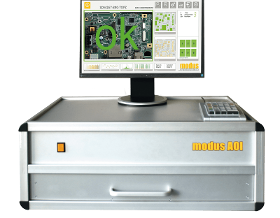
The MLD1200 V2.0-DS is an offline dual AOI system for the inspection of assembled printed circuit boards from both sides at the same time. It has two multi-LED illuminated image scanners as well as our patented parallax-free lenses. It includes modus control units with the latest modus software. An optional Trolley is available. Characteristics: Dual system for double-sided simultaneous inspection for both sides of printed circuit boards. Combination of different inspection tasks such as SMD placement, THT solder joints, conformal coating and full screening for solder beads (solder balls). Capture of any number of barcodes and data-matrix codes on the multi PCB. Shows the test result of both sides at once. Scan range 300 x 400 mm
MODUS HIGH-TECH ELECTRONICS GMBH
Germany
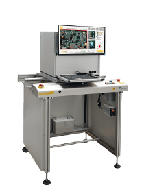
The MLD1200 V2.0-OS is a single-sided offline AOI system for the inspection of assembled printed circuit boards from the top. It has one multi-LED illuminated image scanner as well as our patented parallax-free lenses. It includes a modus control unit with the latest modus software. An optional trolley is available. Characteristics: Single system for inspection printed circuit boards from the top side. Combination of different inspection tasks such as SMD placement, THT solder joints, conformal coating and full screening for solder beads (solder balls). Capture of any number of barcodes and data-matrix codes on the multi PCB. Scan range 300 x 400 mm
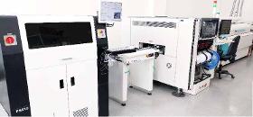
MODUS HIGH-TECH ELECTRONICS GMBH
Germany
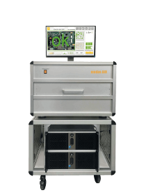
The AOI system is designed for simultaneous inspection of printed circuit boards top and bottom side. It has two multi-LED illuminated scan units with parallax free view. Those systems are also available for single side as for top or bottom view. The system includes complete set of modus control units. The transport module has a length of 1200mm (47.2 in). Characteristics: Double System for dual side simultaneous inspection for printed circuit boards. Simultaneous display of all results of double side inspection. Combination of different inspection tasks such as SMD placement, THT solder joints, conformal coating and full screening for solder beads. Capture of any number of barcodes and data-matrix codes on the multi PCB. Scan range 420 x 530 mm or 300 x 400 mm.
TEPROSA GMBH
Germany
Mechatronic integrated devices or molded interconnect devices (injection-molded circuit carriers) are spatial electronic assemblies – so-called 3D-MID. A special process is used to apply metallic conductor tracks to a specific substrate material (often plastic), thus creating three-dimensional assemblies that also serve as circuit carriers. These spatial electronic assemblies are manufactured using 3D-MID technology and, compared to conventional assemblies, enable the integration of electronic, mechanical, fluidic, optical and thermal functions. The resulting additional benefits represent advantages that cannot be realized with two-dimensional circuit carriers (printed circuit boards).
MODUS HIGH-TECH ELECTRONICS GMBH
Germany
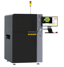
The almost maintenance-free modusAOI MCS18/42-Inline was specially developed for transport conveyor modules in production lines. Existing lines can easily be retrofifitted with this system. The small, cost effective system comes with a 18 or 42 megapixels camera, control unit, modus software and led lighting inclusive controller. Characteristics: Single system for inspection of printed circuit boards from the top side. Combination of diverse application tasks such as SMD placement, pre-reflow, chip control, THT fitting, conformal coating and full screening for lost components. Reads barcodes and data-matrix codes in any position and quantity even on multi-PCBs.
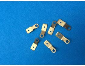
DONGGUAN XINHONGYUAN METAL PRODUCTS LIMITED
China
Hai Tong have high speed press range from 25 to 60 tons utilizing Micron high speed press introduced from Taiwan, We stamp ferrous, non-ferrous, copper based alloys, stainless steel, aluminum,with speeds up to 1500 SPM. We manufacture quality and premier product and we always exceed our customers' expectations. Our progressive die stamping services are perfect for manufacturing components with tight tolerances of +/-0.01mm. We have 15 years of toolings fabrication experience and can consult on any project including failure analysis. We produce pins, copper contact, copper terminal, printed circuit contacts, and much more, which are used on switch, plug,s ocket, computer, household appliance,etc
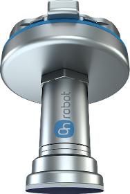
SAMSYS GMBH
Germany
The Gecko Gripper (SP) enables the use of the innovative Gecko adhesive gripper technology in applications with a small surface area. Such areas which could not be automated so far. The gecko-inspired adhesive technology offers precise, track-free gripping. Even with porous workpieces this technology works. For example printed circuit boards or glossy surfaces. Cleaning is not necessary. The three different Gecko Single Pad Grippers (SP1, SP3 and SP5) are named after their payload in kilograms. Of course, the Gecko grippers can be used with leading lightweight robots and cobots. The compact single-pad design allows easy access to the workpiece, even in tight spaces. Since no electronics or air supply is required, the Gecko SP is a cost-effective plug-and-play solution. The Gecko gripper leaves no marks on glass. This eliminates the need for manual cleaning. This means a higher RoI and lower operating costs.
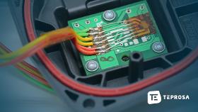
TEPROSA GMBH
Germany
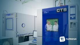
In an environmental simulation, assemblies are subjected to defined environmental conditions to validate their behavior under those conditions. The variables of an environmental simulation test include climatic aspects such as temperature (cold, heat), the air conditions (humidity, wetness), mechanical influences such as dust, vibration, vibration or impacts, and corrosive environmental effects such as salty lift (salt fog). As an environmental simulation laboratory, we simulate these environmental conditions in our climatic chambers and climatic chambers, creating real conditions to investigate the long-term behavior of the test specimens in reality. Environmental simulation and thermal shock testing laboratory for electronic assemblies and printed circuit boards We specialize in performing environmental simulation and temperature shock testing of electronic and mechanical assemblies. With over ten years of experience with the requirements of the automotive industry and medical
TEPROSA GMBH
Germany
We are specialist in strain gage strain measurements on printed circuit boards and all other components. We carry out the application of strain gages and determine for you the actual stresses that occur, or the strain (also strain-rate) on a specific or several components in the manufacturing or assembly process. We perform our DMS measurements with certified measurement technology and according to the specifications of IPC/JEDEC-9704A. Expert advice from TEPROSA When measuring strain, in addition to many factors such as the appropriate measurement technology, it is also important to rperform the strain measurement correctly and to ensure that the sensors record the forces correctly. To ensure that the deformation of an object is correctly determined, it is therefore crucial to select the right strain gauges (also known as measuring strips) and to place them in the correct position on the measured object.
ROTH ELEKTRONIK GMBH
Germany
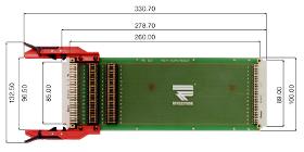
Extender card for 19"-systems DIN 41612 C64 a+c Epoxy fibre-glass FR4 1.50 mm Single-sided 70 µm Cu Solder stop mask Component print Removable short-circuit bridges and two measuring posts for each continuous strip Signalling line pin 2 - 31 Large signalling line pin 1 + 32 Switching voltage 10 mV - 60 V Switching current 0.5 A at 24 V Rest current at 20° C max. 2 A Contact resistance 20 mOhm Extender card: 100% electronically tested Size 100.00 x 278.70 mm (132.50 x 330.70 mm with handle)
VERPET S.R.O.
Czech Rep.
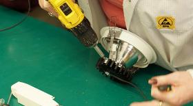
Preparatory, finishing and other required operations are carried out using bench drills and grinders and other small tools. For example, we provide winding of electric motor components. Polishing and polishing of workpieces. soldering of printed circuit boards, soldering, welding
Results for
Printed circuits - Import exportNumber of results
151 ProductsCountries
Company type
Category
- Passive electronic components and printed circuits (66)
- Printed circuits (10)
- Screen printing on metal (8)
- Connectors, electronic (5)
- Moulding, rubber - machinery (5)
- Electronic components (4)
- Monitors, computer (4)
- Laser - cutting and welding machines (3)
- Measurement - Equipment & Instruments (3)
- Building hand tools, non-power (2)
- Chemicals - Basic Products & Derivatives (2)
- Electrical & Electronic Components (2)
- Electronic cards (2)
- Import-export - chemicals and pharmaceuticals (2)
- Ovens, kilns, furnaces and hearths, industrial (2)
- Storage equipment and systems (2)
- Tools & Hardware (2)
- Control boxes - electric (1)
- Automation - systems and equipment (1)
- Automobiles (1)