

OPSIL LTD
Bulgaria

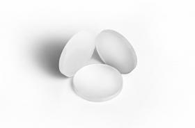
After the surface grinding, the crystal is sliced into wafers with a thickness according to customer’s specifications. Sawing machines with diamond impregnated blade are used for the slicing. We have got 5 sawing machines with a monthly capacity 2500 kg. Maximum diameter Ф152 mm. Wafer thickness up to 80 mm. Slicing accuracy ± 25 microns.
OPSIL LTD
Bulgaria
Wafer thickness(μm) standard >350 >400 >440 >500 minimum 300 350 380 420 Through-the-thickness accuracy(μm) standard ±15 ±20 ±20 ±20 Thickness deviation TTV (μm) maximum 10 15 20 25 standard <7 <10 <10 <12 ИWafer warp (μm) maximum 30 35 40 45 standard <15 <15 <20 <25
NANJING LAB
United Kingdom
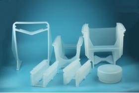
There are many types of wafer carriers, and each has its own application. For example, the front-opening wafer transfer box FOUP can be used in the semiconductor process in the manufacturing plant, the front-opening wafer transport box FOSB can be used for transportation between manufacturing plants, and the wafer flower basket can be used. for wafer cleaning, etc. Fluororesin has an extremely stable molecular structure, so it is hardly affected by light, temperature and chemicals, and is the "king of resins" that subverts the inherent concept. In the process of cleaning chips, high-purity chemicals are required, and fluoropolymers are the only materials that can contain and transport the high-purity chemicals used in the manufacturing process, achieving the extremely high stability and purity required for semiconductor manufacturing.
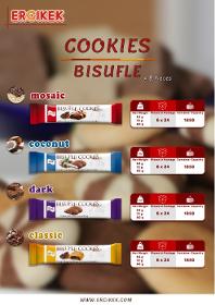
BAK KARDESLER LEBENSMITTELHANDELS GMBH
Germany
Package Quantity : 12 x 700g Artikel Nr: 68205 Grams: 700g
PRECISION SURFACING SOLUTIONS GMBH & CO. KG
Germany
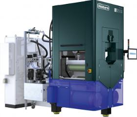
The DW292 is specifically designed for cutting monocrystalline silicon ingots up to 300mm diameter into high quality wafers for the semiconductor industry. The newly developed DW292-300 can be operated with slurry wire, as well as with diamond wire, and has sophisticated features for optimizing warp and ripple. The longer wire field, as well as the higher wire speed and acceleration, enable a higher throughput per machine and year. The use of extremely thin wire is possible thanks to smaller inertia of moving parts, fewer deflection rollers and shorter wire distance. The DW292-300 is highly resistant to temperature fluctuations and vibrations due to its compact and robust machine frame made of mineral casting. Thanks to higher process automation and the new intuitive HMI with dialog-based production wizard, operation is safer, easier and faster.
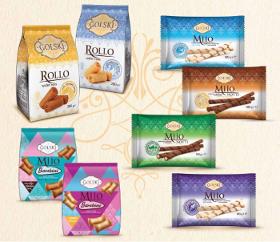
GOLSKI LT
Lithuania
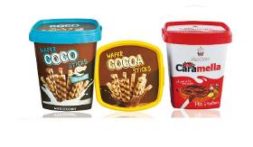
Wafer rolls with different fillings. Fillings: - Hazenut Flavor - Cappuccino Flavor - Vanilla Flavor - Ice-cream Flavor - Cocoa Flavor - Condensed Milk Flavor - Baked Milk Flavor

RIVNE CONFECTIONERY FACTORY
Ukraine
waffles with different flavors: walnut, strawberry, milk, chocolate, lemon, vanilla ...

LARK BISCUITS
Turkey
77 is one of 5 other brands consisting of wafers, biscuits, cakes, marshmallow biscuits........

LARK BISCUITS
Turkey
77 is one of 5 other brands consisting of wafers, biscuits, cakes, marshmallow biscuits...

LARK BISCUITS
Turkey
Voa is one of 5 other brands consisting of wafers, biscuits, cakes, marshmallow biscuits

LARK BISCUITS
Turkey
VOA is one of 5 other brands. Brands consisting of wafers, marshmallow biscuits and cakes.

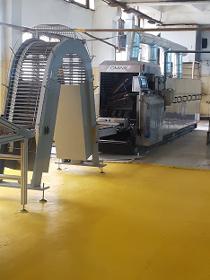
OMAKS MAKINA LTD. STI.
Turkey
Automatic wafer production lines, horizontal flow pack machines and automatic feeding systems for many kind of confectionery products like, chocolate bars, wafers and cakes.
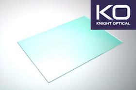
KNIGHT OPTICAL (UK) LTD
United Kingdom
When it comes to a high quality IR Cut filter, it is the substrate with the coating applied that affects the performance. Knight Optical provide high quality wafers for precisely this, and the surface quality of our substrates eliminates blotching at the sensor which occurs on lower quality substrates especially where IR Cut filters are concerned. Our wafers are produced as thin as 500μm & provide exceptional surface quality. However, we can manufacture to a fully customised specification with a wafer thickness as little as 10 μm. Our substrates for stock or custom can be manufactured from a great deal of materials including: •Quartz •Borosilicate •BK7 or equivalent •Sapphire •And many more. Depending on your application for the IR Cut Filter, we can help advise on the best achievable optic for your application. Please read PDF for full specification

KNIGHT OPTICAL (UK) LTD
United Kingdom
Germanium wafers are a semiconductor material & therefore are a smart choice for microelectronics. Due to its unique electric properties, it is widely used for sensors, solar cells and infrared optical applications. The wafers are also great for microelectronics as the space is limited and being available in 500μm or less it makes it perfect to achieve the high quality results required. It’s thermal conductivity makes it a good alternative to silicon. Our stock wafers are produced as thin as 500μm and provide exceptional surface quality. However, we can manufacture to a fully customised specification with a wafer thickness as little as 10 μm. Typical specifications of our germanium wafers are: 10mm – 150mm in diameter <500μm in thickness Doped and undoped Germanium
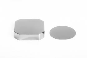
OPSIL LTD
Bulgaria
The company is technologically capable of slicing of thin wafers from optical glass and semi-precious stones.

Do you sell or make similar products?
Sign up to europages and have your products listed

PEEKCHINA CO., LTD.
China
Size: 4", 5", 6", 8", 12" & Non Standard. PEEK handheld tool, a tool for handheld inspection of wafers. PEEK does not contain halogen elements and does not contaminate semiconductor wafers.
XIAMEN INNOVACERA ADVANCED MATERIALS CO., LTD
China
The aluminum nitride (AlN) ceramic has high thermal conductivity(5-10 times as the alumina ceramic), low dielectric constant and dissipation factor, good insulation and excellent mechanical properties, non-toxic, high thermal resistance, chemical resistance ,and the linear expansion coefficient is similar with Si,which is widely used in communication components, high power led, power electronic devices and other fields.Special spec products can be produced upon requests. Product Features: 1.Uniform microstructure 2.High thermal conductivity* (70-180 Wm-1K-1), tailored via processing conditions and additives 3.High electrical resistivity 4.Thermal expansion coefficient close to that of Silicon 5.Resistance to corrosion and erosion 6.Excellent thermal shock resistance 7.Chemically stable up to 980°C in H2 and CO2 atmospheres, and in air up to 1380°C (surface oxidation occurs around 780°C; the surface layer protects the bulk up to 1380°C).

XIAMEN NINESUN IMP. & EXP. CO., LTD
China
Product name: 2-12 Inch Orientation 100/111/110 SSP Prime/Dummy Grade Silicon Wafer Place of Origin: China Material: Silicon Diameter:2-12 inch Thickness: 100-1500um Orientation: 100/110/111 Type/Dopant: intrinsic or P/B or N/Ph Grade: prime/dummy Bow/Warp:<30um TTV:<10um Surface finish: SSP/DSP Supply Ability: 20000 Piece/Pieces per Month Packaging Details:Stardand Package Port of shipment: Xiamen,China Lead Time :25-30days
FEINMETALL GMBH
Germany
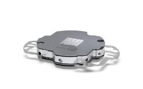
New version of vertical contact technology with focus on increased service life and other advantages.
MICRO-EPSILON
Germany
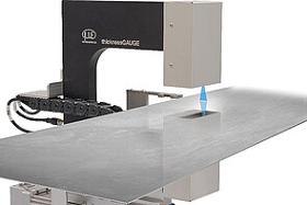
thicknessGAUGE C.LP sensor systems use laser profile scanners for the thickness measurement. These scanners project a laser line onto the surface to be measured. The laser line compensates for strip tilting and enables profile averaging. The laser line measuring technique makes it possible to measure the thickness of structured materials such as embossed surfaces and perforated plates.

MICRO-EPSILON
Germany
The IC2001/USB single-channel converter cable is used for the USB connection of optical sensors equipped with an RS422 interface. The cable is easy to install and can therefore be used in machines and facilities.
OPSIL LTD
Bulgaria
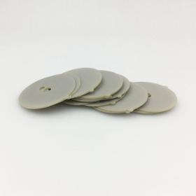
Wafers with maximum dimensions 200x200 mm are being lapped. Capacity – 1000 kg/month. Surface roughness – ˂ Ra 0.1
DISPO PLASTIK LTD
Turkey
Basic Data: Filling Volume: 400 ml Volume Brimful: 460 ml Container Weight: 16 gr Lid Weight: 4 gr Tamper Evidence: Yes Dimensions: Body External Diameter Top : 90 mm Lid External Diameter Top: 90,50 m Body External Diameter Bottom: 64 mm Body Height: 100,10 mm Lid Height: 5,50 mm Raw Material PP/Random Copolymer PP/Block Copolymer IML Decoration: Box: Yes
FEINMETALL GMBH
Germany
Contacting WLCSP, SiP or flipchip wafers requires probe cards that can tolerate high currents while ensuring high signal integrity. The FeinProbe® addresses these applications perfectly.

MICRO-EPSILON
Germany
The IMS5420 is a high-performance white light interferometer for non-contact thickness measurement of monocrystalline silicon wafers. The controller has a broadband superluminescent diode (SLED) with a wavelength range of 1,100 nm. This enables the thickness measurement of undoped, doped and highly doped SI wafers with only one measuring system. The IMS5420 achieves a signal stability of less than 1 nm. The thickness can be measured from a distance of 24 mm.
Results for
Wafers - Import exportNumber of results
59 ProductsCountries
Company type
Category
- Biscuits (6)
- Ceramics, industrial (4)
- Cutting - steels and metals (4)
- SWEETS (3)
- Bread & Cakes (3)
- Confectionary (3)
- Electrical & Electronic Components (3)
- Measurement - Equipment & Instruments (3)
- Sensors (3)
- Industrial valves, operating equipment (2)
- Bottles and containers, insulated - camping equipment (2)
- Handling - Machines & Equipment (2)
- Laser - cutting and welding machines (2)
- Bakery and confectionery industry - machinery and equipment (1)
- Biscuit making (1)
- Ceramics, refractory (1)
- Chemistry - laboratory products (1)
- Chocolates, filled (1)
- Clamp collars, plastic (1)
- Cocoa and chocolate - machines and equipment (1)