
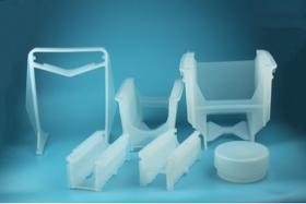
NANJING LAB
United Kingdom
There are many types of wafer carriers, and each has its own application. For example, the front-opening wafer transfer box FOUP can be used in the semiconductor process in the manufacturing plant, the front-opening wafer transport box FOSB can be used for transportation between manufacturing plants, and the wafer flower basket can be used. for wafer cleaning, etc. Fluororesin has an extremely stable molecular structure, so it is hardly affected by light, temperature and chemicals, and is the "king of resins" that subverts the inherent concept. In the process of cleaning chips, high-purity chemicals are required, and fluoropolymers are the only materials that can contain and transport the high-purity chemicals used in the manufacturing process, achieving the extremely high stability and purity required for semiconductor manufacturing.
KNIGHT OPTICAL (UK) LTD
United Kingdom

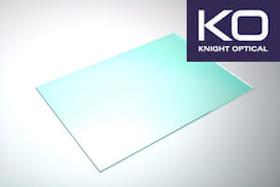
When it comes to a high quality IR Cut filter, it is the substrate with the coating applied that affects the performance. Knight Optical provide high quality wafers for precisely this, and the surface quality of our substrates eliminates blotching at the sensor which occurs on lower quality substrates especially where IR Cut filters are concerned. Our wafers are produced as thin as 500μm & provide exceptional surface quality. However, we can manufacture to a fully customised specification with a wafer thickness as little as 10 μm. Our substrates for stock or custom can be manufactured from a great deal of materials including: •Quartz •Borosilicate •BK7 or equivalent •Sapphire •And many more. Depending on your application for the IR Cut Filter, we can help advise on the best achievable optic for your application. Please read PDF for full specification

KNIGHT OPTICAL (UK) LTD
United Kingdom
Germanium wafers are a semiconductor material & therefore are a smart choice for microelectronics. Due to its unique electric properties, it is widely used for sensors, solar cells and infrared optical applications. The wafers are also great for microelectronics as the space is limited and being available in 500μm or less it makes it perfect to achieve the high quality results required. It’s thermal conductivity makes it a good alternative to silicon. Our stock wafers are produced as thin as 500μm and provide exceptional surface quality. However, we can manufacture to a fully customised specification with a wafer thickness as little as 10 μm. Typical specifications of our germanium wafers are: 10mm – 150mm in diameter <500μm in thickness Doped and undoped Germanium

Do you sell or make similar products?
Sign up to europages and have your products listed
Results for
Wafers - Import exportNumber of results
3 ProductsCountries
Company type