
ADVANCED MAGNETIC TECHNOLOGIES AND CONSULTING (AMT&C)
Russia
The magnetic system of this field source is also built on the principle of nested cylindrical Halbach-structures. An important feature is the presence of two motors, controlled independently, so it is possible to manage the change not only the magnitude but also the direction of the magnetic field. Because the device was designed for operation together with an optical microscope, the vertical size of the system near the working region is reduced to 90 mm. Stepper motors, that turn the two magnetic subsystems, are located on the sides of the casing

ADVANCED MAGNETIC TECHNOLOGIES AND CONSULTING (AMT&C)
Russia
This type of magnetic field sources also is based on the principle of dipole Halbach-structure, but the special design permits to get an optical access to the sample under investigation along several directions with a rather wide aperture. It is possible to supply the system with a built-in field measuring system, connected to a PC. The field adjustment can be controlled from a PC or with a built-in controller. The geometrical and field parameters described above can be change under customer specification.
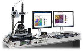
OSTEC ARTTOOL LIMITED COMPANY
Russia
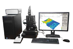
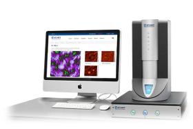
IMOS Interference Microscope-nanoprofilometer enables accurate, quantitative, ISOcompliant noncontact surface measurements and characterization of micro and nanoscale surface characteristics, capturing up to two million data points in seconds. Choosing the right optical profilometer depends on your application requirements, including speed, accuracy, vertical range, automation and flexibility. IMOS optical surface profilometer provides powerful versatility in noncontact optical surface measurements. The system makes it easy and fast to investigate a wide range of surface types, including smooth, rough, flat, sloped and stepped surfaces. All measurements are nondestructive, fast and require no special sample preparation.

OSTEC ARTTOOL LIMITED COMPANY
Russia
SE0S 02 is the best solution for the customers, who need quick analysis, high specifications, safety and fair accuracy of element composition identification results in metal production at minimal purchase, commission and operating of the device costs. Applications: - Industrial analytical laboratories of metallurgical and machine-building factories; - Express analysis of alloys while melting at workshops; - Identification of alloy grade at warehouses; - Research institutes and universities. SEOS 02 identifies the composition of iron alloys (all types of steel and cast iron) and nonferrous alloys on any basis (Al, Cu, Zn, Ni, Ti, Mg, Co, Pb, etc.). CCD allows to analyze the whole range of basic elements used in metallurgy, including S, P, C. SEOS 02 measurement accuracy is in accordance with international regulatory documents. Every SEOS 02 spectrometer passes the state verification procedure as a measuring instrument.

OSTEC ARTTOOL LIMITED COMPANY
Russia
Applications: - Real-time A-scan & A-scan Capture - B-scan & SLICE - Threshold Mapping (post-processing) - Frequency Domain Imaging (FFT) - C-scan with Multi-gate SALI & SALI Groups - Cluster Analysis (post processing) - Advanced Time-of-Flight & Thickness Measurements - Scan Math Before and After Reflow Characterization - 3D Imaging - Void Gating (real-time) Available modes: - A-Scan - Patch Scan - Top Scan - Counterfeit Detection - B-Scan - Focus B - Sub B - Cross B - C-Scan - Dual Gate - SALI - SALI Groups - TX-Scan - Concurrent PE/TX - D-Scan - 3D
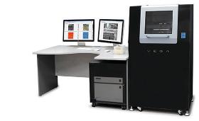
OSTEC ARTTOOL LIMITED COMPANY
Russia
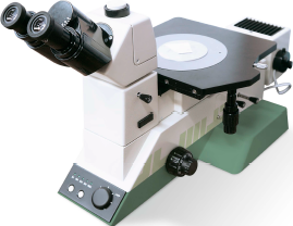
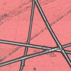
OMOS M series analytical metallographic systems make perfect solutions for the microstructure of materials automatic analysis. When you image and analyze samples, you are often faced with complex and interrupted processes that can make tasks take much longer than you want them to. OMOS M series microscopes have vast experience in bringing together optical precision, automation, analytical power, and data management via the workfloworiented system. The new M series analytical metallographic system product range takes this one step further, offering peerless flexibility and ease of use that can make any task a controlled workflow. Ostec is dedicated to ensuring that the best solutions are available for your work, from microscopes and digital cameras to software and data storage. OMOS M series microscopes bring all of our experience to you, giving you control over every aspect of your hardware, workflow
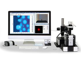
NT-MDT LLC
Russia
Rebirth of Force Spectroscopy Advanced Nanomechanical, Electrical, Optical, Thermal and Piezoresponse Studies Fast Quantitative Nanomechanical Measurements and Force Volume Simultaneous Electrostatic and Nondestructive Conductivity, Piezoresponse and Thermal Studies Advanced CantileverType TipEnhanced Raman Scattering and Scanning NearField Optical Microscopy Topography in Attraction and Repulsive Regimes Young’s Modulus and Force Volume Adhesion and Work of Adhesion Conductivity InPlane and OutofPlane Piezoresponse Temperature and Thermal Conductivity Thermoelectric Electrostatic Kelvin Probe Force, Electrostatic Force and Scanning Capacitance Force Microscopy NearField Component of Optical Response TipEnhanced Raman Scattering In HybriD mode the tipsample distance is modulated according to the quasiharmonic law.
NT-MDT LLC
Russia
Industry leading automation level Outstanding noise floor and thermal drifts Fast scanner with XYZ lownoise closeloop Routine atomic resolution 60+ SPM modes in basic configuration Continuous zoom from millimeter to nanometer range Integrated with new Atomic Force Microscopy technique HybriD Mode™ Atomic Force Microscope NEXT provides motorized sample positioning and integrated high resolution optical microscope positioning, motorized continuous zoom and focusing of the optical microscope. But AFM automation is more than just motorization. Powerful Nova PX software algorithms remove a gap between optics and AFM providing continuous zoom from huge panoramic optical view down to atomic resolution. Since all step movers are coupled together with the optical image, NEXT provides autofocus, fast oneclick cantilever alignment, panoramic optical view and multiple scanning on 5×5 mm range.Cantilever recognition and automatic laser alignment both in liquid and air Autofocus
NT-MDT LLC
Russia
IR s‑SNOM microscopy and spectroscopy with 10 nm spatial resolution Wide spectral range of operation 312 μm Incredibly low thermal drift and high signal stability Versatile AFM with advanced modes SRI (conductivity), KPFM (surface potential), SCM (capacitance), MFM (magnetic properties), PFM (piezoelectric forces) HybriD Mode™ quantitative nanomechanical mapping Integration with microRaman (optional) The ability of s‑SNOM measurements in the visible spectral range (optional) NTMDT Spectrum Instruments presents NTEGRA Nano IR scattering scanning nearfield optical microscope (s‑SNOM) designed for infrared (IR) spectral range. AFM probe is located in the focus of optical system which excites sample structure by IR laser and collects the optical response. Collected light is directed to Michelson interferometer for optical analysis.
NT-MDT LLC
Russia
Highperformance versatile AFM Optical access from top, side and bottom optimized for Raman, TERS and SNOM Flexible optical design providing any combination of excitation/collection configurations Automated AFM laser, probe and photodiode alignment Userfriendly change of wavelength of AFM registration system laser and photodiode Easy and userfriendly change of objectives Integration with IR sSNOM (optional) Since 1998 NTMDT has been successfully integrating AFM with optical microscopy and spectroscopy techniques. More than 30 basic and advanced AFM modes including HybriD ModeTM are supported providing extensive information about the sample surface physical properties. Integration of AFM with confocal Raman/fluorescence microscopy provide the widest range of additional information about the sample. Simultaneously measured AFM and Raman maps of exactly the same sample area provide complementary information about sample physical properties (AFM) and chemical composition (Raman).

NT-MDT LLC
Russia
Early warning and forecasting of the deterioration of engineering materials operating in extreme conditions is a high priority activity within many industrial plants. The ability to perform diagnostics on a plant’s metal work without taking it offline is particularly of high value to industries in the energy, processing and other sectors. Currently diagnostic equipment is only able to discover deterioration in operational pipework and associated equipment after its condition has already reached a dangerous stage of degradation. SOLVER Pipe is a new highprecision and reliable diagnostic system that allows plant managers the ability to decrease risks and achieve incidentfree operation through anticipatory control and scheduled maintenance of materials and equipment within their industrial facilities.Advantage over electron microscopy compact, cheap and does not require complex vacuum technology.
NT-MDT LLC
Russia
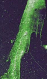
Stateoftheart HybriD 2.0 Control Electronics incorporates highspeed digital lockin amplifiers (LIA) and phase locked loop detector (PLL) for advanced oscillatory resonance modes Amplitude Modulation with Frequency Imaging (AMFI) and Frequency Modulation (FM) modes. They provide exceptional level of spatial resolution of challenging flat and soft samples (selfassembled molecular structures etc.) thanks to ultraprecise control of the tipsample interaction force. Additionally they allow mapping of its mechanical properties. The two images below show topography and probe resonant frequency distribution over lamellar arrangement of short alkane C36H74 on graphite with a spacing of 4.5 nm. One can also see a couple of adsorbates formed on the lamellar surface by disordered alkane chains which are rarely observed by the traditional AM mode.

NT-MDT LLC
Russia
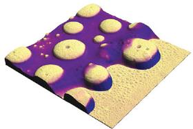
HD Scanning Thermal Microscopy (HD SThM) allows studying local thermal properties simultaneously with QNM measurements. From the hardware point of view it was implemented using AppNano VertiSense™ thermocouple probes. The thermal conductivity and temperature mapping modes (CMM, TMM) can be realized by positioning the AFM laser at the end or the central part of the probe, respectively. HD mode working principle allows exceptional spatial resolution of SThM measurements in comparison to conventional Amplitude Modulation (AM) mode. That was demonstrated in TMM of a microheater sample. SThM and HybriD mode is the winning combination for distinguishing between the constituents of polymer blends as demonstrated in the example of a blend of polystyrene (PS) with low density polyethylene (LDPE) (see below). The difference in thermal conductivity of the polymers (PS – 0.12 W/mK; LDPE – 0.33 W/mK) allows the assignment of the colder matrix to LDPE and the hotter islands to PS.
NT-MDT LLC
Russia
Tip Enhanced Raman Scattering (TERS, nanoRaman) is the technique for enhancement of weak Raman signals and for superresolution Raman imaging with spatial resolution less than 10 nm. As a result of comprehensive research performed together with NTMDT SI customers and partners, we are now able to offer to AFMRaman customers mass produced reproducible TERS probes. TERS imaging requires prolonged tipsample contact at each scanning point but Contact AFM is destructive for both the tip and the sample. Thereby, HD mode is a superior technique for cantilevertype TERS since it noticably increases the tip lifetime and makes possible TERS imaging of soft, loose and fragile samples. Vacuum measurements in amplitude modulation (AM) mode requires unacceptably low scanning speeds because of extremely high Qfactor of AFM probes. Being a nonresonant mode, HD mode allows at least 10 times faster imaging speed.

NT-MDT LLC
Russia
Tip Enhanced Raman Scattering (TERS, nanoRaman) is the technique for enhancement of weak Raman signals and for superresolution Raman imaging with spatial resolution less than 10 nm. As a result of comprehensive research performed together with NTMDT SI customers and partners, we are now able to offer to AFMRaman customers mass produced reproducible TERS probes. TERS imaging requires prolonged tipsample contact at each scanning point but Contact AFM is destructive for both the tip and the sample. Thereby, HD mode is a superior technique for cantilevertype TERS since it noticably increases the tip lifetime and makes possible TERS imaging of soft, loose and fragile samples. Thanks to highspeed HybriD 2.0 Control Electronics the approach and withdrawal optical response signal curve (PMT) can be recorded and processed in realtime. This allows to separate the nearfield from farfield component of optical response and to map it with spatial resolution limited by the tip radius.

NT-MDT LLC
Russia
Thermoelectric studies of nanoscale structures like np junctions, conductive nanowires, graphene oxide etc. are currently of a great interest. HD Scanning Thermoelectric Microscopy (HD SThEM) allows nondestructive mapping of Seebeck coefficient with tip radiuslimited spatial resolution. HD SThEM working principle is based on direct measurement of generated voltage when conductive tip and sample under different temperatures contact each other during fast force spectroscopy measurements.

NT-MDT LLC
Russia
Electrical characterization of objects, that are weakly attached to the surface, has always been a challenge when using standard AFM modes like Conductive AFM. This was because often the tip moved or abraded the objects of interest. HybriD Mode drastically decreased the impact of lateral forces and simplified these experiments. Comparison of conductive and mechanical maps shown in this example allows the clear identification of single nanotubes and bundles. New stateoftheart HybriD 2.0 control electronics allows simultaneous resonant electrostatic studies using twopass technique Kelvin Probe Force Microscopy Electrostatic Force Microscopy Scanning Capacitance Force Microscopy

Do you sell or make similar products?
Sign up to europages and have your products listed
NT-MDT LLC
Russia
Force spectroscopy is a wellknown AFM technique for quantification of local nanomechanical properties. HD mode allows fast, more than 1000 force curves per second measurements, realtime calculation of Young’s modulus according to Hertz, DMT, JKR and other mathematical models and automated cantilever force constant calibration. HybriD Mode uniquely enables stiff materials to be distinguished from each other by means of an AFM probe. Areas corresponding to Bismuth (32 GPa, blue color) and Tin (50 GPa, yellow color) are clearly identified. The mechanical properties map corresponds well with the surface potential image.
NT-MDT LLC
Russia
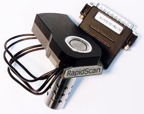
RapidScan™ technology is a combination of mechanical design and highend digital electronical solutions which allows to speed up your AFM by an order of magnitude keeping 90 µm inplane scaninng range. All three access are equipped with highprecision closedloop capacitive sensors.
NT-MDT LLC
Russia
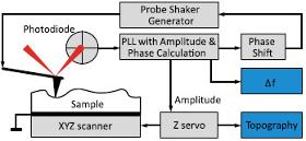
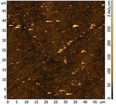
Atomic Force Microscopy is a widely used and powerful technique for investigating materials at a nanoscale range. However, the technique is not simple to use, which elicits varied results between researchers with different levels of experience. NTMDT Spectrum Instruments (formerly NTMDT) have created the intelligent software, ScanT™, inspired by neural networks to make dynamic amplitude modulation AFM (AMAFM) easy for researchers of every skill level. The AFM amplitude modulation (AM) mode, also known as “tapping” or “semicontact”, is based on dependency of cantilever amplitude oscillation on distance between sample surface and tip. This mode is often favored over other AFM modes because it provides minimal impact on the sample and the tip, which can help to preserve both.
NT-MDT LLC
Russia
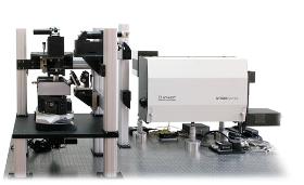
AFM holds a strong positions in scientific research as is used as a routine analytical tool for physical properties characterization with high spatial resolution down to atomic level. Solver Nano is the best choice for scientists who are need a single instrument that is an affordable, robust, userfriendly and professional tool. Solver Nano is designed by the NTMDT SI team that also created High Performance Systems like NTEGRA, NEXT II and NTEGRA Spectra II which have been proven in the scientific community through many key publications. Solver Nano is equipped with a professional 100 micron CL (closed loop XYZ) piezotube scanner with low noise capacitance sensors. Capacitance sensors in comparison with strain gauge and optical sensors have lower noise and higher speed in the feedback signal. The CL scanner is controlled by a professional workstation and software. These capabilities enable all of the basic AFM techniques in compact SPM design.
NT-MDT LLC
Russia
Ultimate imaging quality with buildin acoustic and vibration isolation, active thermostabilization, industry lowest 25 fm/√Hz optical beam deflection sensor noise and unique design of scanningbytip system allow routine high resolution imaging. Equipped with 50+ AFM modes including HybriD mode all cuttingedge nanomechanical, electrical and magnetic studies are available in basic configuration. Automated study of samples arrays by userdefined scenario with database image storage. Up to 200×200 mm and 40 mm in height samples inspection in any point with 1 μm positioning accuracy. Smart ScanT™ software for oneclick optimization of scanning parameters. This is not just an algorithm, it is rather a unique companion that helps a newcomers in AFM to get industry quality images and assists the experts. Wide possibilities of customization integration of addition optical equipment
NT-MDT LLC
Russia
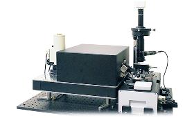
NTEGRA is a multifunctional device for performing the most typical tasks in the field of Scanning Probe Microscopy. The device is capable of performing more than 40 measuring methods, what allows analyzing physical and chemical properties of the surface with high precision and resolution. It is possible to carry out experiments in air, as well as in liquids and in controlled environment. The new generation electronics provides operations in highfrequency (up to 5MHz) modes. This feature appears to be principal for the work with highfrequency AFM modes and using highfrequency cantilevers.* There are several scanning types implemented in NTEGRA scanning by the sample, scanning by the probe and dualscanning. On account of that, the system is ideal for investigating small samples with ultrahigh resolution (atomicmolecular level) as well as for big samples and scanning range up to 100x100x10 µm.
NT-MDT LLC
Russia
AFMSICMRaman triple synergy of powerful nanocharacterization techniques Hopping mode ion conductance microscopy noncontact imaging of living cells and jelly surfaces QNM power of AFM and SICM quantitative nanomechanical studies Smart Patch Clamp automatic nanopipette targeting for ion channel studies HighSpeed LongRange HighResolution mapping at nanoscale Nanoinjection nanopipettes with SICM feedback control can be used for local subpicoliter injections to single cells SICM (Scanning Ion Conductance Microscopy) is an SPM technique which uses nanopipette (sharp glass electrode) for noncontact 3D surface mapping at high resolution. In SICM, the probe to sample distance is controlled via the decrease of ionic current flowing through the tip, as it approaches the sample surface. Biophys.Journ. 73, 653658
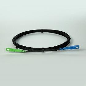
IRIDA LLC (UFANET GROUP)
Russia
Optical patch cord made of DROP cable for outdoor application. Black cable jacket is resistant to temperature drops. Cable lengths are made according to customer's request. Network construction using patch-cords: - Quick and easy installation - Minimum welding - High connection speed - Easy operation - Aesthetics
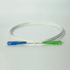
IRIDA LLC (UFANET GROUP)
Russia
The patch cord is designed for indoor installation during connection of the subscribers. Description: Optical patch cord made of DROP cable for indoor application. White cable jacket is resistant to temperature drops. Network construction using patch-cords: - Quick and easy installation - Minimum welding - High connection speed - Easy operation -Aesthetics 1SM SC/APC-SC/APC 5m/10m/15m

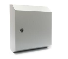
IRIDA LLC (UFANET GROUP)
Russia
Designed for installation in hallways and staircases. Is used for PON networks in apartment buildings. The cabinet can accommodate: – a removable panel for optical terminal boxes or an optical cassette type PLC splitter (130x100x25 mm). – box-type optical coupler (90*20*10) – 2 pcs. – 4 optical adapters SC type. No FOCL welding is required. Up to 8 pcs. of cable slack max 30 cm.
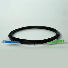
IRIDA LLC (UFANET GROUP)
Russia
The patch cord is designed to be suspended at the overhead line supports during installation of the trunk line, and to connect subscribers. Description: Optical patch cord made of DROP cable for outdoor application. Black cable jacket is resistant to temperature drops. Network construction using patch-cords: - Quick and easy installation - Minimum welding - High connection speed - Easy operation
IRIDA LLC (UFANET GROUP)
Russia
It is applied in private houses during installation of PON networks. The cabinet has 4 slots for placement – removable panel for optical crosses or optical divider cassette type (130x100x25 mm). In addition, the cabinet can accommodate up to 3 ku-1 cassettes for optical fiber welded joints.
Results for
Optical - Import exportNumber of results
60 ProductsCompany type