- europages
- >
- COMPANIES - SUPPLIERS - SERVICE PROVIDERS
- >
- silicon monocrystalline wafers
Results for
Silicon monocrystalline wafers - Import export

MICRO-EPSILON
Germany
The IMS5420 is a high-performance white light interferometer for non-contact thickness measurement of monocrystalline silicon wafers. The controller has a broadband superluminescent diode (SLED) with a wavelength range of 1,100 nm. This enables the thickness measurement of undoped, doped and highly doped SI wafers with only one measuring system. The IMS5420 achieves a signal stability of less than 1 nm. The thickness can be measured from a distance of 24 mm.
Request for a quote
OPSIL LTD
Bulgaria
Resistance for mirrors
Request for a quote
PEEKCHINA CO., LTD.
China
Size: 4", 5", 6", 8", 12" & Non Standard. PEEK handheld tool, a tool for handheld inspection of wafers. PEEK does not contain halogen elements and does not contaminate semiconductor wafers.
Request for a quote
NANJING LAB
United Kingdom
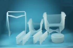
There are many types of wafer carriers, and each has its own application. For example, the front-opening wafer transfer box FOUP can be used in the semiconductor process in the manufacturing plant, the front-opening wafer transport box FOSB can be used for transportation between manufacturing plants, and the wafer flower basket can be used. for wafer cleaning, etc. Fluororesin has an extremely stable molecular structure, so it is hardly affected by light, temperature and chemicals, and is the "king of resins" that subverts the inherent concept. In the process of cleaning chips, high-purity chemicals are required, and fluoropolymers are the only materials that can contain and transport the high-purity chemicals used in the manufacturing process, achieving the extremely high stability and purity required for semiconductor manufacturing.
Request for a quoteDo you sell or make similar products?
Sign up to europages and have your products listed
Results for
Silicon monocrystalline wafers - Import exportNumber of results
4 ProductsCountries
Company type