
ZIMMER GMBH KUNSTSTOFFTECHNIK
Germany

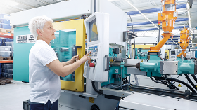
When it comes to sophisticated plastic injection molding, we are completely in our element. We process all common thermoplastics, from standard to high-performance plastics. A fully automated production with handling systems for part removal and QA tests guarantees an economic production of your parts. We also have experience with the overmolding of various inserts such as threaded bushings, electronic contacts, circuit boards and much more. This and much more are the reasons why we are a reliable partner for almost all industries: Automotive industry aerospace industry Mechanical engineering Medical technology Construction industry Electrical engineering Jewelry and watch industry Furniture industry
TEPROSA GMBH
Germany
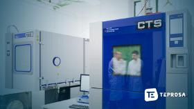
In an environmental simulation, assemblies are subjected to defined environmental conditions to validate their behavior under those conditions. The variables of an environmental simulation test include climatic aspects such as temperature (cold, heat), the air conditions (humidity, wetness), mechanical influences such as dust, vibration, vibration or impacts, and corrosive environmental effects such as salty lift (salt fog). As an environmental simulation laboratory, we simulate these environmental conditions in our climatic chambers and climatic chambers, creating real conditions to investigate the long-term behavior of the test specimens in reality. Environmental simulation and thermal shock testing laboratory for electronic assemblies and printed circuit boards We specialize in performing environmental simulation and temperature shock testing of electronic and mechanical assemblies. With over ten years of experience with the requirements of the automotive industry and medical
DR.-ING. MAX SCHLÖTTER GMBH & CO. KG.
Germany
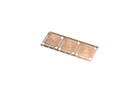
The smallest electronic components, such as chips or connectors, present special challenges for electroplating coatings. In addition to the conductor pattern construction in the manufacturing of printed circuit boards, copper processes are used for filling blind microvias (blind holes) and metallizing through holes. Good metal distribution is necessary even with unfavorable geometry. The most important application areas are found in the automotive industry, telecommunications, and consumer goods industry, but also in the field of e-mobility.
KRAMSKI GMBH
Germany
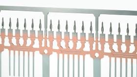
The press-fit connection provides an enduring mechanical and electrical connection between the printed circuit board and plug connectors. The Compliant Pin has many applications and our customers use them in a wide variety of products, including sensor and radar casings, electronic controllers, plug connectors, printed circuit board connectors and more. Advantages: — no complex soldering process — high mechanical stability — repairable — gas-tight connection at the point of contact
TOPCOD DEUTSCHLAND GMBH & CO. KG
Germany
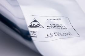
Aluminum composite foil bags, also known as aluminum vacuum bags, are produced in our production from highquality raw materials on fully automatic production lines and are characterized by the following properties Antistatic Waterproof Electrostatic shield Heat sealable The size of the bags is not fixed by default but rather can be implemented individually for our customers also as a 3in1 solution including tailormade desiccant and moisture indicator. Style and size are variable, such as flat bags, 3D bags, etc. The production takes place in strict accordance with the standards GB / T 10371988, GB / T 10382000, MILB81705C. Packaging of electronic components Packaging of printed circuit boards (PCB Packaging of integrated circuits (IC) Packaging of hard drives

Do you sell or make similar products?
Sign up to europages and have your products listed

BERATRONIC GMBH
Germany
Technical data •Max. Panel size up to 1500mm x 670mm •PCB thickness from 0.1-17.5mm •Smallest hole 0.075mm •Smallest trace/spacing 50µm •Copper layer up to 1000µm •Number of layers up to 58 •Aspect Ratio 20:1 •Rigid flex and flex •Viaplugging •Impedance control •Laser Microvias •Blind, Buried Vias Basic material •FR4, FR4 High TG, FR4 •halogen-free, CEM1/3, Rogers, •Ceramic (Al2O3), polyimide and others Surface •HAL lead-free, HAL Pb/Sn, chem. Ni/Au (ENIG), chem. Ni/Pd/Au (ENEPIG), chem. Sn, chem. Ag, OSP(Entek), galv. Ni/Au, Carbon, Ag/Pt (thick film technology) and others Solder resist and placement printing •Different paint systems (including halogen-free) and colors Standards •ISO 9001:2015 / IATF 16949 •UL listing •RoHS / REACH •Manufacturing according to IPC A600 class 2 and 3 Delivery times •Rush service from 1 AT •Series from 10 AT Data preparation •Legacy document preparation •Scan Service •Data conversion •CAM data preparation •CAD layout service

BERATRONIC GMBH
Germany
Our services •Layout creation •Material procurement •SMD assembly •Manual and semi-automatic •Mounting •Reflow and wave soldering •Selective soldering •Automatic Optical Inspection (AOI) •X-ray inspection •System assemblies •In circuit tests and •Function test •Revision and repair •Rework Station •Short delivery times
Results for
Electronic circuit boards - Import exportNumber of results
8 ProductsCountries
Company type