Laser structuring of interconnection circuits on...
Description
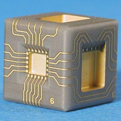
Laser ablation technology helps the engineer to develop circuit carriers which cannot be manufactured with chemical etching technology. This kind of product results from combining the technologies of precision-grinding of ceramics and laser ablation of metallised thin-film layers. We name this concept "three-dimensional interconnection circuit or CI3D". Principle The laser structuring consist to etch directly a metallization layer deposited on a ceramic carrier with a laser beam without using a mask. This is called laser micromachining or laser ablation - because metal is ablated. Laser ablation allows patterns to be etched directly on the ceramics substrate, very rapidly and beam displacements to be programmed limitless. Equipment Solid-state lasers are mostly used for micromachining applications because they feature precision, speed and selective etching. We currently use a Nd :YAG laser with 60 W output. It enables us to etch thin-film metallised layers with thickness of up...
Documents
Request for quotes
Create one request and get multiple quotes form verified suppliers.
- Only relevant suppliers
- Data privacy compliant
- 100% free